جميع الكتب

مهني

1 Markets I: The Ecosystem and Exchange-Traded Marketsالأسواق عبر الإنترنت 2 Markets II: Rates, FX and Creditالأسواق عبر الإنترنت 3 Markets III: Commodities, Energy and Cryptoالأسواق عبر الإنترنت 4 Quantitative Methodsالأساليب عبر الإنترنت 5 Derivatives and Volatilityالمشتقات عبر الإنترنت 6 Rates, Credit, XVA and Riskالفائدة والائتمان والمخاطر عبر الإنترنت 7 Research Craft: Predictors, Backtests, Measurement, Portfoliosالبحث عبر الإنترنت 8 Strategies I: Equities and Futuresالاستراتيجيات عبر الإنترنت 9 Strategies II: Volatility, Relative Value, Macro and the Bank Desksالاستراتيجيات عبر الإنترنت 10 Microstructure and Executionالتنفيذ عبر الإنترنت 11 Market Making and High-Frequency Tradingصناعة السوق عبر الإنترنت 12 Machine Learning for Marketsتعلم الآلة عبر الإنترنت 13 Low-Latency Softwareالتكنولوجيا عبر الإنترنت 14 Networks, Hardware and Trading Infrastructureالتكنولوجيا عبر الإنترنت 15 Research, Data and Risk Platformsالتكنولوجيا عبر الإنترنت 16 The Desk and the Firmالشركة عبر الإنترنت 17 The Industry: Firms, Roles and Careersالمسارات المهنية عبر الإنترنت 18 The Interview Bookالمسارات المهنية عبر الإنترنت
التطبيقات حول المدرب تسجيل الدخول ابدأ القراءة

Quantitative Finance · المسرد

ما معنى Clock domain crossing؟

Definition 6.7 Networks, Hardware and Trading Infrastructure · الفصل 6 — Programmable Hardware I: Architecture and Toolchain

A clock domain crossing is a signal passing between parts of a design clocked by unrelated clocks; it must go through a synchroniser or an asynchronous FIFO, or it will sometimes be sampled while it changes.
Model: a decision of 12 levels of logic split into registered stages (0.5\, n s per level, 0.4\, n s per register, model values). Left: the maximum clock, against the clocks two line rates require; right: the latency at that clock. Five stages are no better than four, because 12/5 = 12/4 = 3. Data: fig_fpga.py.
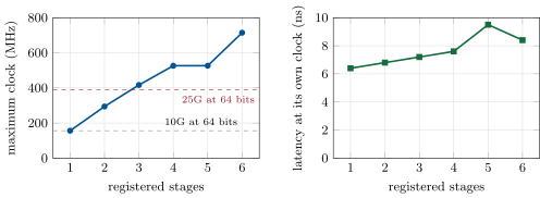
Figure 6.2. Model: a decision of 12 levels of logic split into registered stages (0.5 ns0.5\,\mathrm{n}\mathrm{s} per level, 0.4 ns0.4\,\mathrm{n}\mathrm{s} per register, model values). Left: the maximum clock, against the clocks two line rates require; right: the latency at that clock. Five stages are no better than four, because ⌈12/5⌉=⌈12/4⌉=3\lceil 12/5\rceil = \lceil 12/4\rceil = 3. Data: fig_fpga.py.
اقرأ في الفصل →