Networks, Hardware and Trading Infrastructure · Technology
6Programmable Hardware I: Architecture and Toolchain
A Ethernet link delivers a design its bytes at ten billion bits a second; a design that takes them 64 bits at a time must accept a word every , at 156.25 MHz. A design built of registers and logic between them takes a fixed number of those cycles to decide, and it takes that number every time: no cache miss, no interrupt, no scheduler, no garbage collector sits between the last byte of a price and the decision. Determinism, rather than raw speed, is what programmable hardware sells to a trading firm, and it is bought with a different way of writing programs.
This chapter introduces the devices, the languages and the tools, and writes a first design: a field extractor that pulls a price out of a frame while the frame is still arriving, simulated cycle by cycle in two independent simulators and checked against a Python model. Chapter 7 builds the trading designs on top of it.
6.1 The fabric: logic blocks, memories, transceivers and clocks
Definition 6.1 (Field-programmable gate array, configurable logic block)
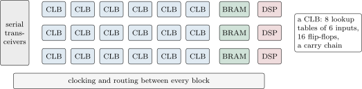
A field-programmable gate array (FPGA) is a chip whose logic and wiring are configured after manufacture by loading a configuration file: an array of small programmable logic elements, memories, arithmetic blocks and serial transceivers, joined by programmable routing. A configurable logic block is the array’s repeated logic element: a group of lookup tables, each of which computes any Boolean function of a few inputs by looking it up in a small memory, with flip-flops to register their outputs and a carry chain for arithmetic.
Definition 6.2 (Block RAM)
A block RAM is a dedicated on-chip memory of a few tens of kilobits, of which an FPGA has hundreds or thousands, each readable and writable in one clock cycle, typically through two independent ports.
The resources are concrete. In AMD’s UltraScale family each configurable logic block holds eight 6-input lookup tables and sixteen flip-flops, with an 8-bit carry chain, and each block RAM holds 36 kilobits, usable as one memory or two independent halves. A 6-input lookup table computes any function of six bits in one level of logic; a function of more bits needs several tables in several levels, and the depth of that tree of levels, together with the wiring between the tables, sets how fast the design can be clocked. Beside the logic sit the serial transceivers, which turn the optical module’s bit stream into parallel words, and the clocking resources, which distribute clocks and let parts of the design run at different rates.
6.2 Describing hardware: register-transfer level and high-level synthesis
Definition 6.3 (Register-transfer level, hardware description language)
A design written at register-transfer level (RTL) describes, for every clock cycle, how the values held in registers are computed from the registers’ previous values and the inputs, through combinational logic. A hardware description language (Verilog, SystemVerilog, VHDL) is a language in which such designs are written: its statements describe circuits that all operate at once, not instructions executed in order.
Definition 6.4 (Logic synthesis, place and route)
Logic synthesis translates an RTL description into a network of the device’s primitives (lookup tables, flip-flops, memories). Place and route assigns each primitive to a location on the chip and chooses the programmable wires between them; its result is the configuration file loaded into the device.
Definition 6.5 (High-level synthesis)
High-level synthesis (HLS) compiles a function written in C or C++ into an RTL design, choosing its registers and schedule; the designer steers it with directives such as the pipeline’s initiation interval, the number of cycles between successive inputs (an interval of one accepts a new input every cycle).
The difference in thinking is the chapter’s first lesson. A C++ loop over the eight bytes of a word runs eight times, one after the other; the same loop in SystemVerilog describes eight copies of its body that all exist and all compute in the same cycle. Listing 6.1 is the combinational heart of the field extractor: for each of the beat’s eight byte lanes it asks whether that byte belongs to the field and, if so, shifts it into the value, all in one cycle. What would be a data-dependent branch in software becomes a set of multiplexers whose delay does not depend on the data.
  always_comb begin
    acc_next  = acc;
    done_next = 1'b0;
    for (int i = 0; i < 8; i++) begin
      pos = int'(base) + i;
      if (keep[7 - i] && pos >= OFF && pos < OFF + LEN) begin
        acc_next = (acc_next << 8) | {56'd0, data[63 - 8 * i -: 8]};
        if (pos == OFF + LEN - 1) done_next = 1'b1;
      end
    end
end6.3 Timing closure: clock periods, critical paths and pipelining
Definition 6.6 (Critical path, timing closure)
The critical path of a synchronous design is its slowest path from one register to the next: the delay of its logic and wiring plus the registers’ own overhead, which sets the shortest clock period the design supports. Timing closure is the work of making every register-to-register path fit within the target clock period.
Definition 6.7 (Clock domain crossing)
A clock domain crossing is a signal passing between parts of a design clocked by unrelated clocks; it must go through a synchroniser or an asynchronous FIFO, or it will sometimes be sampled while it changes.
Proposition 6.8 (What pipelining buys)
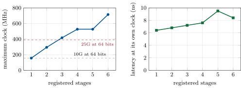
Let a decision need levels of logic of delay each, and let a register add . Split into registered stages of at most levels, the design’s clock period is and its latency is . Pipelining raises the maximum clock and never lowers the latency: .
Proof. Each stage is one register-to-register path of at most levels, so the period is its delay. The decision crosses stages, one period each, and . ∎
The proposition explains a design choice that looks backwards: a trading design adds registers, and cycles, to go faster. The line sets the clock. A link taken 64 bits at a time needs 156.25 MHz; a link at the same width needs 390.625 MHz. A decision that fits in one cycle at the first clock may need three cycles at the second, and its latency in nanoseconds then rises a little while the design keeps up with a link two and a half times as fast. Figure 6.2 draws the trade-off with model delays of per level and per register, stated as model values: a real device’s delays come from its timing reports.
fig_fpga.py. if (PIPE == 0) begin : g_flat
always_ff @(posedge clk) begin
out_valid <= rst ? 1'b0 : in_valid;
le <= a <= thresh;
end
end else begin : g_two
logic [3:0] lt, eq;
logic v1;
always_ff @(posedge clk) begin
v1 <= rst ? 1'b0 : in_valid;
out_valid <= rst ? 1'b0 : v1;
for (int s = 0; s < 4; s++) begin
lt[s] <= a[16 * s +: 16] < thresh[16 * s +: 16];
eq[s] <= a[16 * s +: 16] == thresh[16 * s +: 16];
end
// most significant slice decides unless equal, and so on down
le <= lt[3] | (eq[3] & (lt[2] | (eq[2] & (lt[1] | (eq[1] & (lt[0] | eq[0]))))));
end
end
endmodule6.4 Simulation and verification
Definition 6.9 (Testbench, cycle-accurate model)
A testbench is the code that drives a design’s inputs in simulation and checks its outputs. A cycle-accurate model is a software model of a design that reproduces its outputs cycle by cycle, used as a reference against which the hardware is checked, and as a fast stand-in for it.
A design is verified long before it is synthesised, because a synthesised design is slow to build and hard to observe. This book simulates every design in two independent tools. Verilator compiles the SystemVerilog into a C++ model driven by a C++ testbench: it is a compiler rather than a traditional simulator, and fast. Icarus Verilog interprets the same source under a SystemVerilog testbench. The two testbenches read the same stimulus and print the same event lines, and the test compares them cycle for cycle and against a Python golden model; a disagreement between the simulators is a bug in the design (usually an ambiguity the language permits) before it is a bug in either tool. The designs are written for the versions installed here (Verilator 4.038, Icarus Verilog 11) and for their newer releases, and the tests fail, rather than skip, when a simulator is missing.
| Cycle | Input accepted | Outputs registered at the end of the cycle |
|---|---|---|
| 0 | beat 0: bytes 10–17 | — |
| 1 | beat 1: bytes 18–1f, last | — |
| 2 | — | field 16171819; CRC-32 f4a7fd67 |
| 3 | — | comparison (one stage): at most the threshold |
| 4 | — | comparison (two stages): at most the threshold |
hdk_top in Verilator, no back-pressure: a 16-byte frame of bytes 10 to 1f, the field at bytes 6 to 9, the threshold equal to the field. The skid buffer registers each accepted beat; the field and the CRC are registered the cycle after the beat that completes them. Icarus prints the same cycles. Data: nw_fpga.first_frame.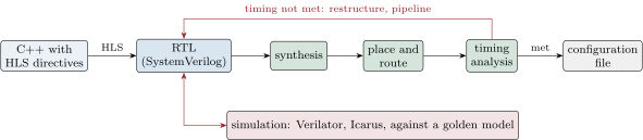
6.5 Smart network cards
Definition 6.10 (SmartNIC)
A SmartNIC is a network interface card with its own programmable processing (an FPGA, or processors) between the network ports and the host, so that packets can be parsed, filtered, timestamped, answered or generated on the card without reaching the host.
For a trading firm the FPGA card is where hardware meets the rest of the system: its transceivers terminate the exchange’s links, its logic decodes and decides, and its bus connects it to the host’s software, which configures it and receives what it has seen. A design on such a card reads the frame as it arrives, before the last byte is in, which is what the table of this chapter shows at small scale: the field is known the cycle after the beat that completes it, while the rest of the frame is still to come. Chapter 7 decides on it.
6.6 Tutorial: a field extractor in two simulators
Goal. Simulate the first design cycle by cycle in Verilator and Icarus, check both against a Python model under random back-pressure, and model what pipelining costs. End state: Table 6.1, Figure 6.2 and the green tests of firm.hdlkit.
- Read the design.
hdl/hdk_top.svchains a skid buffer, the field extractor (Listing 6.1), a CRC-32 unit and the comparator (Listing 6.2). - Build both.
firm_hdlkit.build_verilatorrunsverilator –cc –exe –buildwith the C++ testbench;build_icarusrunsiverilog -g2012with the SystemVerilog one. - Run and compare.
write_stimturns frames into 8-byte beats,write_readygives the downstream’s back-pressure; both simulators print the same event lines, andgoldencomputes the fields, CRCs and comparisons in Python. - Cycles and clocks.
nw_fpga.first_framegives the table;timinganddepth_forevaluate Proposition 6.8, andpython fig_fpga.pywrites the chart’s data.
What to change next. Move the field to bytes 60 to 63 and read the cycle it appears in; set the downstream ready to 50% and count the cycles the whole stream takes.
6.7 Build: the hardware toolkit
Purpose. The primitives and the verification harness every hardware design of this book uses.
Interface. SystemVerilog modules hdk_skid (skid buffer, parameter W), hdk_field (OFF, LEN), hdk_crc32, hdk_cmp (PIPE) and hdk_top; testbenches tb/hdk_tb.cpp (Verilator) and tb/hdk_tb.sv (Icarus) printing the same event lines. Python firm_hdlkit: require, beats, write_stim, write_ready, build_verilator, build_icarus, run_verilator, run_icarus, events, golden, CycleModel.
Rules. Beats of 8 bytes, byte 0 in the most significant lane; every output registered; the HDL is accepted by Verilator 4.038 with -Wall and by Icarus 11 with -g2012, without warnings; a missing simulator raises ToolMissing.
Acceptance tests. code/firm/hdlkit/tests/: both simulators identical cycle for cycle and equal to the golden model on random frames with random back-pressure, for one- and two-stage comparators; every beat accepted once; the latencies in cycles; the beat and golden functions by hand.
Stretch. An asynchronous FIFO for a clock domain crossing and a test that samples it at unrelated clocks; a wider (512-bit) beat.
Sources and further reading
- AMD, UltraScale Architecture Configurable Logic Block User Guide (UG574) and Memory Resources (UG573); AMD, Vitis High-Level Synthesis User Guide (UG1399).
- Verilator documentation; Icarus Verilog documentation; IEEE 1800 (SystemVerilog).
- J. W. Lockwood and co-authors, “A Low-Latency Library in FPGA Hardware for High-Frequency Trading (HFT)”, IEEE Symposium on High-Performance Interconnects (2012).
6.8 Exercises
Exercise 6.1 ★
What clock does a design need to take a link 32 bits at a time, and 128 bits at a time?
Solution
Solution of Exercise 6.1.
MHz at 32 bits; MHz at 128 bits.
Exercise 6.2 ★
With the model delays, what is the maximum clock of a decision of 12 levels in one stage, and its latency?
Solution
Solution of Exercise 6.2.
Period : 156.25 MHz, and one cycle of latency, .
Exercise 6.3 ★
In Table 6.1, at which cycle would the field appear if it were at bytes 12 to 15? And at bytes 14 to 17 of a 24-byte frame?
Solution
Solution of Exercise 6.3.
Bytes 12 to 15 lie in beat 1, like bytes 6 to 9’s last bytes: still cycle 2. Bytes 14 to 17 end in beat 2 (bytes 16 to 23), accepted at cycle 2: the field is registered at cycle 3.
Exercise 6.4 ★★
Why does the loop of Listing 6.1 take one cycle whatever the data, while the same loop in C++ may not?
Solution
Solution of Exercise 6.4.
The SystemVerilog loop is unrolled into eight byte lanes that exist side by side; every lane is evaluated in every cycle, and the result is selected by multiplexers whose delay is fixed. The C++ loop runs its iterations one after the other, with branches whose cost depends on the data and the predictor, and on a machine shared with other work.
Exercise 6.5 ★★
In Figure 6.2, why is six stages faster than five? What does that say about counting levels?
Solution
Solution of Exercise 6.5.
Six stages leave levels per stage, five leave 3, the same as four: only the deepest stage counts, so levels must divide evenly across stages for a new stage to help. Designers count levels on the critical path, not in total.
Exercise 6.6 ★★
What does the skid buffer do that a single register cannot, and what would happen to the stream without it when the downstream stalls?
Solution
Solution of Exercise 6.6.
It holds the beat that is already in flight when the downstream stalls, so the upstream can see a registered ready (no combinational path through the stage) without losing data. With a single register and a registered ready, the beat sent in the cycle the stall is seen would be overwritten or dropped.
Exercise 6.7 ★★★
Coding. Build hdk_top with the field at offset 10 and length 8 in both simulators, run the tests’ random frames, and check both against the golden model. How many cycles after the completing beat does the field appear?
Solution
Solution of Exercise 6.7.
Both simulators agree with the golden model. The field (bytes 10 to 17) ends in beat 2; it is registered the cycle after the skid buffer registers that beat, as for the chapter’s field.
Exercise 6.8 ★★★
Find the flaw. “The design passes in Verilator, so it will work on the card; running a second simulator is redundant.”
Solution
Solution of Exercise 6.8.
The two simulators interpret the language independently; a design that relies on an ordering the language leaves open (blocking assignments across processes, reading a signal in the same cycle it is written) can pass one and fail the other, and fail again on the chip. A disagreement is cheap to find in simulation and expensive on the card; neither simulator replaces timing analysis either.
6.9 Problem: Eight Cycles
Problem 6.1
Weekend problem — a decision against a line’s clock
A firm’s hardware decision (parse a field, compare it with a threshold, check a limit) needs 12 levels of logic. Use the chapter’s model: per level, per register. The design takes the line 64 bits per cycle.
Part I — The clocks.
- What clock does a line require at 64 bits a cycle? A line?
- What is the maximum clock of the decision in one stage?
- Does it meet either line’s clock?
- How long does a 128-byte frame take to arrive at each line’s clock, in cycles and nanoseconds?
Part II — Pipelining.
- How many stages does the line require?
- What is the maximum clock with that many stages?
- What is the latency of the decision when the design runs at the line’s clock?
- What is the latency at the design’s own maximum clock?
Part III — Where the time goes.
- If the field ends at byte 40 of a 128-byte frame, how many beats must have arrived for the field to be complete?
- Add the decision at the clock: when is the decision made, counted from the frame’s first bit?
- How much of the frame is still arriving at that moment?
- Why is it worth deciding before the frame’s check sequence arrives, and what is the risk?
Part IV — The verdict.
- State the named result: the pipeline depth that meets the clock and the decision’s latency, against the unpipelined design at its own clock.
- Would a 128-bit datapath change the answer?
- What would a real design’s timing report replace in this model?
- Why does pipelining never reduce latency?
- Why may the firm accept a longer decision latency for a faster line?
- How would you verify the pipelined design against the unpipelined one?
- What does a clock domain crossing add if the decision runs at a clock other than the line’s?
- In one sentence: what does the line’s rate decide about the design?
Solution
Solution of Problem 6.1.
- 156.25 MHz and 390.625 MHz.
- MHz.
- The line’s exactly, with no margin; not the line’s.
- 16 beats: at 156.25 MHz, at 390.625 MHz.
- Three: levels, a period.
- 416.7 MHz.
- .
- .
- Byte 40 is in the sixth beat (bytes 40 to 47): six beats.
- Six beats and three stages, nine cycles at : .
- Nine of sixteen beats have arrived: seven beats, 56 bytes, are still to come.
- The decision is ready before the frame ends; waiting for the check sequence would add those nanoseconds. The risk is acting on a corrupted frame, which the design must be able to cancel or must accept as rare.
- Named result. Three stages meet 390.625 MHz, and the decision takes at the line’s clock, against for the unpipelined design at its own 156.25 MHz, which cannot keep up with the faster line at this width.
- Yes: at 128 bits the line needs 195.3125 MHz, which two stages meet (294 MHz), for a latency of at the line’s clock, in fewer, wider beats.
- The delay per level and per register, and the routing delays, path by path.
- Each stage is at least as long as its logic, and the stages’ periods are set by the deepest one.
- Because a design that cannot keep up with the line loses data or needs a wider datapath, and a few nanoseconds of decision are worth less than seeing every message.
- Run both on the same stimulus in both simulators and compare their outputs, shifted by the extra cycles.
- A synchroniser or FIFO between the clocks: a few cycles of latency and a source of rare, hard-to-reproduce errors if done wrong.
- It sets the clock, and the clock sets how much logic each cycle may hold.
6.10 Interview questions
Interview question 6.1 ★ developer
What is an FPGA, and why do trading firms use them?
Solution
Solution of Interview question 6.1.
A chip of programmable logic, memories and transceivers configured by a file: the design is a circuit that processes the network stream as it arrives, in a fixed number of cycles, with no operating system or scheduler in the way. Firms use it where determinism and the last hundreds of nanoseconds matter: feed handling, filtering, risk checks, and triggered orders.
What the interviewer is looking for: determinism and processing on the fly, not only speed.
Interview question 6.2 ★★ developer
What is timing closure? What do you do when a path fails timing?
Solution
Solution of Interview question 6.2.
Making every register-to-register path fit the clock period. On a failing path: pipeline it (add a register), restructure the logic (fewer levels, use the carry chain or a memory), reduce fan-out, constrain placement, or lower the clock if the line allows.
What the interviewer is looking for: the critical path and the concrete fixes.
Interview question 6.3 ★★ developer
Pipelining adds cycles. How can it make a design faster?
Solution
Solution of Interview question 6.3.
It shortens each stage, raising the clock, so the design keeps up with a faster line or accepts a new input every cycle. The latency of one decision does not fall; throughput and the ability to meet the line’s clock rise.
What the interviewer is looking for: latency against throughput and the line’s clock.
Interview question 6.4 ★★ developer
RTL or high-level synthesis for a trading design? Argue both sides.
Solution
Solution of Interview question 6.4.
RTL gives cycle-exact control of the critical path and the latency, which the fastest designs need. HLS writes and changes faster, lets software engineers contribute and explores trade-offs quickly, at the cost of less control over the schedule and harder debugging of what the compiler produced. Many teams use HLS for the less critical blocks and RTL for the hot path.
What the interviewer is looking for: control against productivity, block by block.
Interview question 6.5 ★★★ developer
How would you verify a hardware feed parser before it runs against a live exchange?
Solution
Solution of Interview question 6.5.
A golden model in software; simulation in two simulators against recorded and synthetic feeds, including gaps, bursts and malformed frames, with random back-pressure; property checks (no message lost or duplicated); then hardware-in-the-loop replay of recorded captures and comparison of the card’s output with the software handler’s.
What the interviewer is looking for: a reference model and replay of real captures, not only unit tests.
Interview question 6.6 ★★ developer
What is a clock domain crossing, and what goes wrong if it is not handled?
Solution
Solution of Interview question 6.6.
A signal passing between unrelated clocks: sampled while it changes, a flip-flop can go metastable and different bits of a bus can be sampled on different sides of a change. It needs a synchroniser for single bits and an asynchronous FIFO or handshake for data; the failures are rare and irreproducible.
What the interviewer is looking for: metastability and the standard structures.