University Physics — Year 3 · Bachelor Year 3
24Electrons in Solids
Copper conducts electricity a million billion billion times better than quartz — the widest range of any physical property, commanded by materials that look like grey lumps either way. The scaffolding of the last chapter explains none of it; the electrons poured into it explain all of it. This chapter runs the century’s three passes at the problem, each inheriting the last’s wreckage: Drude’s classical pinball (1900), which gets Ohm’s law right and the heat capacity scandalously wrong; Sommerfeld’s Fermi gas, which is Chapter 19 cashing its cheque; and Bloch’s insight that an electron wave in a periodic lattice Bragg-reflects like any other wave — opening band gaps that sort all solids into metals, insulators, and the narrow-gap middle children, semiconductors, on which the whole electronic age is built. The chapter ends inside a solar panel.
24.1 Drude’s pinball metal
Proposition 24.1 (The Drude conductivity)
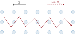
Treat a metal’s valence electrons as a classical gas, density , bouncing off obstacles every seconds. A field accelerates each between collisions; the average drift velocity is , tiny beside the thermal motion. The current density then obeys Ohm’s law locally, , with
Copper’s measured demands — and the model’s two glories follow: it explains why resistors heat (the field’s work is thermalised each collision), and it predicts the Wiedemann–Franz law, that is the same constant for all metals — electrons carry both charge and heat (Exercise 24.5).
Proof. Between collisions ; starting afresh at each collision, the mean velocity acquired in a mean time is . Then . ∎
Remark 24.2 (Sommerfeld’s rescue)
Drude’s gas should add per electron to a metal’s heat capacity; experiment finds a hundred times less. Chapter 19 already acquitted the electrons: they are a degenerate Fermi gas, , and only the thermal shell within of the Fermi surface can respond — to heat, and to scattering. Sommerfeld’s re-run of Drude with Fermi–Dirac statistics keeps the conductivity formula (with now the lifetime of Fermi-surface electrons, whose is , not thermal speed), fixes the heat capacity to its measured sliver, and even repairs Wiedemann–Franz’s numerical constant. One mystery survives every free-electron model: why quartz will not conduct at all.
24.2 Bloch: the lattice speaks
Theorem 24.3 (Bloch states and band gaps)
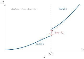
In a perfect periodic potential, the stationary states are Bloch waves — plane waves dressed with the lattice’s own periodicity — which propagate without scattering: a perfect crystal has zero resistance, and real resistance comes from imperfections (vibrations, impurities). But not all energies survive. At the electron’s wavelength is : Bragg’s condition on the lattice itself (Theorem 23.6 made the same discovery for sound). The reflected and incident waves form two standing patterns — charge piled on the ions (lower energy) or between them (higher) — so the free-electron parabola tears open: an interval of forbidden energies, the band gap , separates a filled-out band of allowed states from the next. A crystal’s electronic identity is its ladder of bands and gaps.
Proof. Admitted at this level. ∎
Definition 24.4 (Metals, insulators, semiconductors)
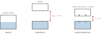
Fill the bands with the crystal’s electrons, two per state (Chapter 14), coldest first. If the topmost occupied band is partly filled, infinitesimal energy can shift electrons into net motion: a metal (sodium: one valence electron, half a band; divalent metals conduct through overlapping bands). If it is exactly full, with a wide gap above, no small push can rearrange anything: an insulator (diamond, ). If the gap is small — in silicon — thermal agitation hoists a few electrons across, each leaving a mobile hole below: a semiconductor, whose carrier count doubles every few degrees. Hence the great divide: metals conduct worse when heated (more vibrations to scatter off), semiconductors better (exponentially more carriers) — one sign flip that identifies a material’s class in a single measurement.
24.3 Engineering the gap: doping and the junction
Definition 24.5 (Doping)
Replace one silicon atom in a million by phosphorus (five valence electrons): four bonds are satisfied and the fifth electron, bound by a mere (Exercise 24.10), is free at room temperature. Such donors make an n-type semiconductor, conduction by electrons; boron (three electrons) is an acceptor, grabbing a bond electron and releasing a mobile hole — a missing electron that moves, responds to fields, and carries positive charge as genuinely as a bubble carries buoyancy: p-type. Doping swings the carrier density — and hence conductivity — across six orders of magnitude at will: the knob that turns sand into circuitry.
Proposition 24.6 (The p–n junction)
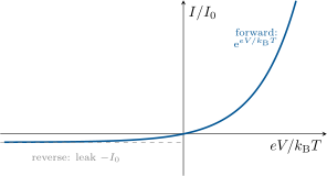
Join p-type to n-type. Electrons spill toward the holes and annihilate them near the interface, exposing a depletion zone of fixed ionised dopants whose double layer builds an internal field — equilibrium at the built-in voltage in silicon. The junction then rectifies: forward bias lowers the barrier and current grows as ; reverse bias raises it and only a leakage flows:
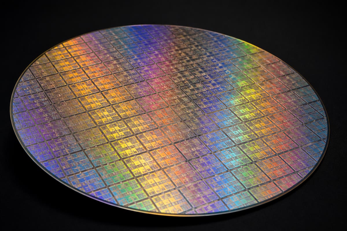
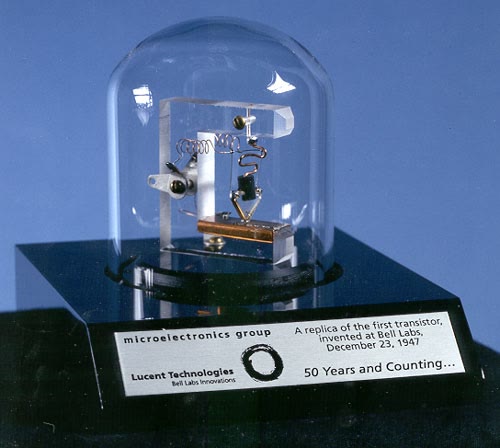
This asymmetry is the diode — and, run in its variants, the LED (recombining pairs emit gap-energy photons), the solar cell (gap-energy photons create pairs that the built-in field sweeps out: Problem 24.1), and, doubled into sandwiches, the transistor: the switch of which a modern chip prints hundreds of billions.
Proof. Admitted at this level. ∎
24.4 Exercises
Exercise 24.1 ★
Drude’s copper. , resistivity . Compute (a) ; (b) the mean free path using the Fermi velocity ; (c) that path in lattice constants (); (d) explain why so long a flight already hints that ions themselves do not do the scattering.
Solution
Solution of Exercise 24.1.
(a) . (b) . (c) About 110 lattice constants. (d) An electron sailing past a hundred ions without scattering cannot be bouncing off the ions themselves — the lattice must be transparent to it, exactly what Bloch’s theorem (Theorem 24.3) later proves.
Exercise 24.2 ★
The snail in the wire. A copper wire carries . (a) Compute the drift velocity. (b) How long would an electron take to cross a lamp cord? (c) Why does the lamp nevertheless light instantly? (d) Compare with and comment on Drude’s pinball picture.
Solution
Solution of Exercise 24.2.
(a) — under a millimetre per second. (b) About 23 minutes. (c) The field establishes itself along the wire at nearly light speed and sets the whole electron sea drifting at once: the marchers are slow, the order to march is not. (d) : conduction is an imperceptible bias on a violent quantum motion, not a calm classical flow.
Exercise 24.3 ★
Sorting by bands. Classify, with the band-filling rule: (a) sodium (one valence electron); (b) magnesium (two — yet a metal: what must its bands do?); (c) diamond (); (d) silicon () — and state for each the sign of .
Solution
Solution of Exercise 24.3.
(a) Half-filled band: metal, . (b) Two electrons would fill its band exactly — magnesium conducts because its full band overlaps the next empty one: metal, . (c) Full band, gap: insulator (formally , but with essentially no carriers to count). (d) Semiconductor: , the exponential sign flip that betrays the class.
Exercise 24.4 ★
Gaps and photons. (a) What photon wavelength matches silicon’s gap, and in which spectral region does silicon become transparent? (b) Same for diamond: why is it clear in the visible? (c) A gallium nitride LED has : what colour edge does that set, and why did blue LEDs need this material? (d) Why does a red LED die dark rather than glow faintly white when overdriven?
Solution
Solution of Exercise 24.4.
(a) : silicon is transparent in the infrared beyond that — which is why infrared cameras can be lensed in silicon. (b) , in the ultraviolet: no visible photon can be absorbed, so diamond is water-clear. (c) : a gap wide enough for blue () exists in nitrides and almost nowhere else practical — the blue LED waited decades on materials growth. (d) Its gap fixes its photon: overdriving adds heat, not gap width, and the diode cooks dark — an LED’s colour is a material constant, not a brightness setting.
Exercise 24.5 ★★
Wiedemann–Franz. (a) From copper’s and at , compute . (b) Compare with the Sommerfeld value . (c) Explain in one sentence why one kind of carrier ties the two conductivities. (d) Cooking pans and their handles: use the law to explain a kitchen’s material choices.
Solution
Solution of Exercise 24.5.
(a) . (b) Within ten percent of . (c) The same Fermi-surface electrons carry both the charge and the heat, so their scattering time cancels in the ratio. (d) The steel pan conducts heat to the food because its electrons move; the wooden handle, an insulator in both senses, keeps them — and the heat — out of your hand.
Exercise 24.6 ★★
The heat-capacity acquittal. (a) Drude predicts from the electrons: with copper’s , what fraction would that add to the lattice’s (one conduction electron per atom)? (b) Chapter 19 instead gives : evaluate the suppression at (). (c) Why does the electronic term nevertheless win at liquid-helium temperatures (recall the lattice’s )? (d) What measurement, plotted as against , untangles the two?
Solution
Solution of Exercise 24.6.
(a) Fifty percent extra — flagrantly absent from experiment. (b) : the electronic term is throttled to under a percent. (c) The lattice’s collapses faster than the electrons’ : below a few kelvin the “negligible” electrons are all that is left. (d) : the intercept weighs the electrons, the slope the lattice — one graph, both tenants.
Exercise 24.7 ★★
The Fermi surface meets the zone. (a) For copper, compute the Fermi wavelength with . (b) Compare with : how close is the Fermi surface to the Bragg condition? (c) Explain physically why the two standing waves at (charge on ions versus between them) must differ in energy. (d) Which experimental fact of Exercise 24.1 does Bloch’s no-scattering theorem finally explain?
Solution
Solution of Exercise 24.7.
(a) : . (b) : the same order — copper’s Fermi surface reaches toward the zone boundary, and the gap-opening physics happens at the energies that matter. (c) One standing wave piles its charge on the positive ions (lower electrostatic energy), the other between them (higher): same wavelength, two energies — the gap. (d) The 110-lattice-constant free path: Bloch waves do not scatter off a perfect lattice, so only vibrations and impurities remain to resist.
Exercise 24.8 ★★
The exponential thermometer. Intrinsic silicon has . (a) Compute the carrier-density ratio between and . (b) Hence sketch a thermistor’s resistance against temperature and contrast it with a platinum wire’s. (c) Why the factor 2 in the exponent (what is created in pairs)? (d) Estimate the temperature at which silicon electronics fails because intrinsic carriers swamp a doping ().
Solution
Solution of Exercise 24.8.
(a) : . (b) The thermistor’s resistance plunges exponentially — a steep, sensitive curve; platinum’s climbs gently and linearly (more phonons). One is a thermometer by carrier count, the other by scattering. (c) Carriers are born in electron–hole pairs, and the equilibrium splits the gap’s cost between the two — hence . (d) reaches near : the doping drowns and the circuit forgets its design. Real devices give up earlier — their reverse leaks, doubling every ten kelvin, misbehave first.
Exercise 24.9 ★★
Doping arithmetic. Silicon has . (a) One phosphorus per million silicon atoms: what carrier density, and what ratio to ? (b) By what factor has one ppm of dirt changed the conductivity? (c) Explain why semiconductor fabrication first purifies to parts per billion before doping deliberately. (d) Estimate the average distance between donors and compare with the orbit of Exercise 24.10.
Solution
Solution of Exercise 24.9.
(a) — five million times . (b) The same factor : one speck per million atoms owns the conductivity outright. (c) Because accidental ppm would do the same uninvited: only a crystal pure to ppb has a conductivity that belongs to the designer. (d) , ten times the orbit: donors are isolated hydrogens; push the doping a hundredfold and the orbits touch — an impurity band, and eventually a metal.
Exercise 24.10 ★★★
The donor as a hydrogen atom. The fifth phosphorus electron orbits its ion inside silicon: screen Coulomb by (Chapter 22) and lighten the electron to its effective band mass . (a) Scale the hydrogen results of Chapter 11: show and evaluate. (b) Compare with at : are donors ionised? (c) Scale the Bohr radius the same way. (d) The orbit spans dozens of lattice cells: explain why that self-consistently justifies using and at all.
Solution
Solution of Exercise 24.10.
(a) (the measured phosphorus value, , keeps the scale honest). (b) Comparable to : essentially all donors are ionised at room temperature — the premise of Definition 24.5. (c) . (d) An orbit spanning dozens of cells sees the crystal as a smooth medium — which is precisely the condition under which a bulk and a band-averaged are legitimate: the approximation certifies itself.
Exercise 24.11 ★★★
Junction numbers. A silicon diode has , , . (a) Compute . (b) From the diode law, compute the ratio of currents at and . (c) Why does — hence the reverse leak — roughly double every ? (d) A bridge of four such diodes turns AC into DC: sketch the circuit’s idea in words.
Solution
Solution of Exercise 24.11.
(a) . (b) : ratio — the diode is a one-way street to eight digits. (c) : the same exponential as Exercise 24.8, hence the rule-of-thumb doubling. (d) The four diodes form a diamond: each half-cycle, whichever pair is forward-biased steers the current through the load in the same direction — AC in, bumpy DC out.
Exercise 24.12 ★★★
Designing the solar gap. (a) Photons below pass through; photon energy above is lost as heat within picoseconds. Explain the resulting trade-off in choosing . (b) The optimum near caps single-junction efficiency at about a third (Shockley–Queisser): where does silicon () stand? (c) Why do tandem stacks (a wide-gap cell atop a narrow-gap one) beat the cap? (d) Why is a hot solar panel a worse one? (Two chapter-honest reasons: the diode law’s , and the gap’s slight shrinkage with .)
Solution
Solution of Exercise 24.12.
(a) Narrow the gap and more photons clear it but each delivers only the small gap energy; widen it and each photon pays more but fewer qualify: harvest voltage peaks in between. (b) Just below the optimum: silicon’s ideal ceiling is — close enough that its cheapness wins. (c) The wide-gap top cell takes the blue at high voltage, passing the red to the narrow-gap cell below: each photon is harvested near its own energy, thermalisation shrinks, and the stack’s ceiling climbs toward the forties. (d) Heat raises exponentially, dragging down the open-circuit voltage ; and the gap itself narrows slightly, trading voltage for current it cannot fully recover.
24.5 Problem: The rooftop referendum
Problem 24.1
The rooftop referendum. Your neighbour is deciding whether to roof their house with photovoltaic panels and has appointed you, the physicist, as arbiter. The candidate panel: silicon, , sixty cells in series, rated under the standard of noon sunlight.
Part I — Sunlight meets the gap.
- Sunlight is roughly a thermal spectrum (Chapter 20): compute the energy of its peak photons (Wien) in eV.
- Silicon’s gap is : what is the longest wavelength a silicon cell can harvest?
- Roughly a fifth of the sun’s power arrives in photons below the gap. What happens to it in the panel?
- A green photon is absorbed: how much of its energy survives as electron–hole pair energy, and where does the rest go, and how fast?
- Combine items 3 and 4 into the spectrum’s verdict: about half the incident power is gone before any electronics begins. State the two loss channels in one sentence each.
- Why does a photon need at all — what forbids absorbing two half-gap photons in quick succession in ordinary silicon?
Part II — The junction as engine.
- Each cell is a p–n junction. Explain in three sentences how the depletion zone’s built-in field turns a created pair into external current — which carrier goes which way, and why they do not simply recombine.
- With and , compute at .
- A working cell delivers about . Sixty in series: the panel’s operating voltage?
- From the rating, deduce the operating current.
- Estimate the photon flux (photons per second) the panel absorbs usefully, taking per absorbed photon, and compare with the electron flux your current implies: what fraction of absorbed photons yields a collected electron?
- The rated efficiency: from incident. Reconcile 20 % with Part I’s “half lost before electronics”: where do the remaining thirty points go?
- Why does the cell deliver and not the full of the gap? (Name the culprit in the diode law.)
Part III — Real roofs.
- A cloudless winter noon at latitude delivers light at elevation. Compute the geometric factor relative to normal incidence on a horizontal panel.
- The panel datasheet lists of output: a black roof panel reaches in summer. How much of the rating survives?
- Explain the temperature loss with Exercise 24.12(d).
- A chimney shades one cell of the sixty. Why can that strangle the whole series string — and what does the cell’s own diode nature do to the poor shaded cell?
- Manufacturers wire a bypass diode across each sub-string: explain its job in one sentence.
- Averaged over days and weather, the roof yields of rated power. Estimate the yearly energy from the panel in kilowatt-hours.
Part IV — The verdict.
- At per kWh, what does the panel earn per year? With an installed cost of , what is the payback time?
- The panel took roughly to manufacture (silicon is purified by melting): how long until it has repaid its own energy?
- Your neighbour asks why the panel cannot be “just made black” to catch the sub-gap fifth. Answer with band theory in two sentences.
- They ask next why not stack a second, smaller-gap panel beneath: answer with Exercise 24.12(c) — and name the practical catch.
- Thirty years on, the panel has faded to 85 % of its rating. Which microscopic villains of this chapter (recall what limits , and what junctions fear) plausibly age a cell?
- Deliver the arbiter’s summary in four lines: gap physics sets the harvest, the junction converts it, series wiring and temperature tax it, and the ledger — energy and euros — closes in the panel’s favour.
Solution
Solution of Problem 24.1.
1. : about . 2. . 3. It sails through the cells (no final state to absorb into) and ends as heat in the backing — warming the roof, not the wires. 4. survives as the pair; the excess drains into phonons within picoseconds — faster than any circuit could intercept. 5. Sub-gap transparency ( of the power) and above-gap thermalisation (): the spectrum is taxed half before the junction sees a single electron. 6. Absorption is a single-photon quantum jump needing a real final state; at half the gap there is none to pause in, and two-photon events are negligible at sunlight’s photon densities. 7. Pairs created in or near the depletion zone feel the built-in field: electrons are swept to the n side, holes to the p side, and the field separates them faster than they can find each other to recombine — charge accumulates until an external circuit relieves it as current. 8. . 9. . 10. . 11. Panel-wide, above-gap light is at each: photons per second — but the sixty cells are in series, so the (an electron flux ) passes through each cell, whose own share of photons is per second: nearly every absorbed photon yields a collected electron. The quantum efficiency is excellent; the losses are energetic, not numeric. 12. After the spectrum’s 50 %, the cell pays the voltage deficit () and a few points of reflection and recombination: , trimmed to the rated 20 %. 13. The leakage : the open-circuit voltage stops where photocurrent and diode leak balance — about , well short of the gap. 14. : half the noon rating from geometry alone — before clouds. 15. : , leaving — the sunniest days are not the best days per watt. 16. Heat inflates exponentially, and the open-circuit voltage — a logarithm’s rebuke — falls a fraction of a percent per kelvin; the slightly shrunken gap finishes the job. 17. Series wiring forces one common current: the shaded cell, generating none, is driven into reverse bias by its fifty-nine colleagues and dissipates their power as a hot spot — the string throttles to the weakest cell. 18. The bypass diode gives the current a forward path around the shaded sub-string, sacrificing its voltage instead of the whole panel’s output. 19. per year. 20. per year: payback in roughly years, then two decades of profit. 21. one year: the panel repays its manufacturing energy about as fast as its price. 22. Blackness is not a choice but a band structure: absorption needs an empty state one photon-energy above a full one, and below the gap silicon simply has none to offer — paint cannot add states. 23. Stack a wide-gap cell on top to take the blue at high voltage and pass the red down: the tandem beats the single-junction ceiling. The catch: the series stack must match currents (and prices) between layers. 24. Whatever shortens and poisons junctions: UV-created defects and in-diffused impurities scatter and trap carriers, moisture corrodes contacts, and hot spots age the diodes — the slow entropy of a crystal asked to sit in the sun for thirty years. 25. The gap harvests half the sun; the junction turns pairs into of ordered current; series strings, shade and summer heat take their cut; and at a year against a one-year energy and three-year money payback, the arbiter rules: roof it.