University Physics — Year 1 · Bachelor Year 1
10The Operational Amplifier
A strain gauge glued to a bridge girder changes its resistance by a thousandth when a truck passes; the Wheatstone bridge around it (Chapter 6) turns that into two millivolts. Two millivolts drive nothing. Between the gauge and the alarm that will close the bridge to traffic sits a chip the size of a fingernail, sold for a few cents, which multiplies the signal by a thousand, filters it, compares it with a threshold and lights a lamp — four jobs, one component, four different wirings. This chapter introduces the operational amplifier through its ideal model, derives the handful of circuits that every instrument is built from, and shows what happens when the feedback is removed.
10.1 The component and its ideal model
Definition 10.1 (Operational amplifier)
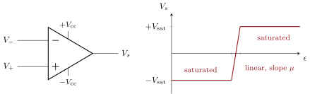
An operational amplifier is an integrated circuit with two inputs — the non-inverting input at potential and the inverting input at — and one output at potential , powered by two supplies (typically ) that are usually left off the diagrams. It amplifies the difference :
with an open-loop gain of order and a saturation voltage slightly below . When would exceed , the output sticks at or : the saturated regime.
Definition 10.2 (Ideal operational amplifier)
The ideal model assumes: (i) no current enters either input, (infinite input impedance); (ii) the output imposes its voltage whatever the current drawn (zero output impedance); (iii) infinite gain, . In the linear regime () the third assumption forces
the two inputs sit at the same potential (a “virtual short circuit”) although no current flows between them.
Proposition 10.3 (Negative feedback and the linear regime)
If the output is connected back to the inverting input through a network (negative feedback), the circuit has a stable linear operating point at and the ideal-amplifier rules apply. If the output is fed back to the non-inverting input (positive feedback), or not fed back at all, the amplifier saturates: according to the sign of .
Partial proof. With negative feedback, suppose rises a little above its equilibrium value; through the feedback network rises, falls, and the amplifier pulls back down: the perturbation is corrected. With positive feedback the same perturbation raises , increases and drives further away until it saturates. The full argument (a first-order model of the amplifier, , and the stability of the resulting differential equation) is the subject of the Year 2 volume; the rule above is what one uses. ∎
Remark 10.4 (Real amplifiers)
Three departures from the ideal matter in practice. The open-loop gain falls with frequency as with : the product (the gain–bandwidth product) is the bandwidth available to a follower, and a circuit of closed-loop gain has bandwidth . The output cannot change faster than the slew rate, . And a small input offset voltage () is amplified like a signal — fatal for millivolt inputs unless trimmed.
10.2 The basic linear circuits
Method 10.5 (Analyzing an ideal op-amp circuit in the linear regime)
- Check that the feedback goes to the inverting input.
- Write : the input nodes obey Kirchhoff’s node law with no current into the amplifier (dividers and Millman’s theorem apply).
- Write and solve for .
- Verify afterwards that ; if not, the amplifier is saturated and the result is .
Proposition 10.6 (Follower, non-inverting and inverting amplifiers)
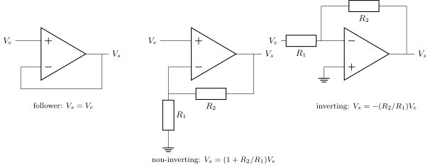
- Follower: output wired to , input on : ; infinite input impedance, zero output impedance.
Non-inverting amplifier: output to through a divider (feedback) and (to ground), input on :
Inverting amplifier: grounded, input through to , feedback from output to :
with held at ground potential (a virtual ground) and an input impedance .
Proof. Follower: and ; gives . Non-inverting: no current into , so the divider gives ; equate to . Inverting: ; node law at with : . The source delivers : input impedance . ∎
Example 10.7 (Why a follower)
A sensor of Thévenin resistance feeding a load delivers only of its open-circuit voltage (Remark 6.14). A follower between them draws no current from the sensor and drives the load from a zero-impedance output: the full voltage arrives. The follower is an impedance adapter — and it makes the cascade rule of Proposition 9.14 exact.
Proposition 10.8 (Summing and difference amplifiers)
Inputs through to the inverting node, feedback , grounded:
With through to (feedback ) and through to (with from to ground):
Proof. Summing: node law at the virtual ground, . Difference: (divider); node law at : , so ; set and simplify. ∎
10.3 Integrator and differentiator
Proposition 10.9 (Integrator)
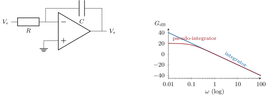
Input through to , a capacitor as feedback, grounded:
The gain falls per decade at every frequency and the phase is : an exact integrator — until the smallest offset or bias, integrated forever, drives the output into saturation.
Proof. Virtual ground: the current flows into the capacitor, whose voltage (from to the output) is ; hence , and in complex notation . ∎
Remark 10.10 (Taming the integrator)
A resistor in parallel with gives
a first-order low-pass of DC gain and cutoff , which integrates for but cannot drift to saturation. Likewise the differentiator (capacitor at the input, resistor as feedback: , ) amplifies high-frequency noise without limit unless a small series resistor caps its gain.
Example 10.11 (Triangle from square)
, , . A square wave of gives a triangle of slope and amplitude — without the attenuation of a passive RC, and with a zero-impedance output to feed the next stage.
10.4 Active filters
Proposition 10.12 (First-order active low-pass)
The inverting amplifier with a capacitor across its feedback resistor has
a low-pass of DC gain (which can exceed ) and cutoff , with zero output impedance — stages cascade by simple multiplication.
Proof. Inverting amplifier with the feedback impedance in place of . ∎
10.5 Without negative feedback: comparators
Proposition 10.13 (Comparator)
With no feedback, the ideal amplifier is saturated: if , if . With a reference on one input and a signal on the other, the output tells whether the signal exceeds the reference — a one-bit converter.
Proof. exceeds for any . ∎
Proposition 10.14 (Schmitt trigger)
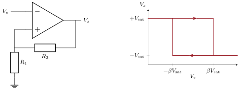
Feed a fraction of the output back to (divider to ground, from the output) and apply the signal to . The output switches from to when rises past , and back when falls below : two thresholds, a hysteresis of width , immune to noise smaller than that width.
Proof. Positive feedback: saturated. If then , and stays positive until exceeds ; then the output flips, drops to , and the new state holds until falls below that. ∎
Example 10.15 (The relaxation oscillator)
Connect the Schmitt trigger’s output back to its own inverting input through , with from to ground. The capacitor charges toward and flips the trigger each time it reaches : the output is a square wave, the capacitor voltage a chain of exponential arcs, and the period is
(Exercise 10.12): for . No input, one capacitor, and a clock — a system that oscillates because it cannot settle, a theme that returns with the feedback oscillators of the Year 2 volume.
10.6 Exercises
Exercise 10.1 ★
A non-inverting amplifier has , , . Gain? Output for ? Largest input before saturation?
Solution
Solution of Exercise 10.1.
; ; saturation at .
Exercise 10.2 ★
An inverting amplifier has , . Gain, input impedance, current drawn from a source, output.
Exercise 10.3 ★
A sensor of internal resistance and open-circuit voltage must drive a load. Voltage across the load without and with a follower between them?
Solution
Solution of Exercise 10.3.
Without: divider , . With the follower: — the follower draws nothing from the sensor and supplies the the load needs.
Exercise 10.4 ★
A summing amplifier has and inputs through and . Write ; compute it for , .
Solution
Solution of Exercise 10.4.
.
Exercise 10.5 ★★
Derive the difference amplifier’s . With , , , : output? What happened to the common to both inputs?
Solution
Solution of Exercise 10.5.
; at : , so ; with : . Numbers: ; the common contributes nothing — common-mode rejection.
Exercise 10.6 ★★
Integrator with , , output initially zero. A step is applied: slope of the output and time to saturation (). A square wave of : shape and amplitude of the output.
Solution
Solution of Exercise 10.6.
: slope ; saturation after . Square wave: triangle of amplitude (plus whatever constant the initial charge left).
Exercise 10.7 ★★
A resistor is added across the capacitor of the previous integrator. Give the transfer function, the DC gain, the cutoff frequency, and the gain at ; in which range does the circuit still integrate?
Solution
Solution of Exercise 10.7.
: DC gain ; cutoff ; at , , — the integrator value . It integrates for .
Exercise 10.8 ★★
Design an inverting active low-pass with a gain of in the passband and a cutoff at , using .
Solution
Solution of Exercise 10.8.
: ; .
Exercise 10.9 ★★
A real amplifier has and . For a non-inverting amplifier designed for a gain of : actual DC gain (keep finite in the analysis), and bandwidth. Bandwidth of a follower?
Solution
Solution of Exercise 10.9.
With finite : , , so . Bandwidth ; follower: .
Exercise 10.10 ★★★
A comparator with on watches a slowly rising signal carrying of noise. Describe the output as the signal crosses . Remedy?
Solution
Solution of Exercise 10.10.
Each noise excursion across flips the output: a burst of rapid switching (“chatter”) around the crossing. Remedy: hysteresis wider than the noise, i.e. a Schmitt trigger.
Exercise 10.11 ★★★
Schmitt trigger with , , : derive and compute the two thresholds. Sketch for a triangular of amplitude .
Solution
Solution of Exercise 10.11.
: thresholds . The output is while rises until , flips to , stays there until falls below , flips back: a square wave of the triangle’s frequency, its edges at the threshold crossings.
Exercise 10.12 ★★★
Relaxation oscillator with (). Derive the period from the charging of through between the two thresholds; choose for with ; sketch and .
Solution
Solution of Exercise 10.12.
With , charges from toward : , reaching when : half-period , hence . : ; , . : square wave ; : exponential arcs between .
10.7 Problem: An instrumentation chain for a strain gauge
Problem 10.1
Weekend problem — from two millivolts on a bridge girder to a red lamp: followers, a difference amplifier, an active filter and a Schmitt trigger, and the two imperfections that decide whether the chain works
A strain gauge of resistance , , , forms a Wheatstone bridge with three fixed resistors, fed by . The bridge output (between the two midpoints) is (the sign is chosen by wiring). Amplifiers: ideal unless stated; ; where needed, , slew rate , input offset .
Part I — The bridge and its loading.
- Recall why for small .
- Compute at full scale ().
- Give the potential of each midpoint (relative to the bridge’s negative terminal) at zero strain and at full scale. What is their common value called?
- Each midpoint is the output of a divider of two resistors: what is the Thévenin resistance seen between the two midpoints?
- An amplifier whose input resistance is is connected across the bridge output: what fraction of does it receive?
- Why does a follower on each midpoint cure this? State the two properties used.
- What are the followers’ output voltages (in terms of , ), and what current do they draw from the bridge?
Part II — Amplifying the difference.
- The followers feed a difference amplifier ( at both inputs, as feedback and to ground). Derive .
- Choose and for a gain of .
- A second, non-inverting stage multiplies by : give its resistors, the total gain, and the output at full scale.
- Both midpoints sit near (the common-mode voltage). What does an exactly matched difference amplifier do with it? If one resistor ratio is off by , estimate the spurious input-referred voltage and compare with the signal.
- The first amplifier has a input offset. What output error does it produce after the total gain? Conclude.
- With , what is the bandwidth of each stage? Is it sufficient for a signal below ?
- The output must swing by when a truck arrives in about : does the slew rate limit?
Part III — Filtering. The amplified signal carries a hum picked up from the mains.
- Design an inverting active low-pass with gain and cutoff , using : find .
- Compute its attenuation at in decibels.
- Compute the phase shift at and the corresponding delay. Acceptable for an alarm?
- Why is an active filter preferable here to a passive RC (two reasons)?
- A second identical stage is cascaded: attenuation at ? Why is the product rule exact here?
Part IV — Threshold and alarm. The alarm must trip when the strain exceeds .
- To what output voltage of the chain does this correspond? A comparator with this reference: output states.
- The filtered signal still carries of noise near the threshold. What does the plain comparator do?
- A Schmitt trigger with the reference on one input and feedback : show that the thresholds are ; choose for and give , .
- State the two thresholds in volts and in strain.
- The output drives an LED (, ) through a resistor: compute it. What protects the LED when the output is at ?
- Summarize the chain, stage by stage, and name the two non-idealities that set its real limits.
Solution
Solution of Problem 10.1.
1. Two dividers: (Proposition 6.22); wiring fixes the sign.
2. .
3. always; at full scale. The shared by both is the common-mode voltage.
4. Each midpoint: ; between the two midpoints, .
5. : a loss.
6. Infinite input impedance (no current from the bridge, so the midpoints keep their open-circuit potentials) and zero output impedance (the next stage can draw what it needs).
7. and exactly; zero current.
8. As in Proposition 10.8: , node law at , .
9. .
10. : e.g. and . Total gain ; full scale .
11. Matched: the common cancels exactly (only survives). A mismatch passes about of it: an input-referred error of order , ten times the full-scale signal — the four resistors must be matched to better than (or the common-mode voltage removed first).
12. , forty percent of full scale: unusable without offset trimming, a low-offset (chopper) amplifier, or a zero calibration with no load on the girder.
13. Stage 1: ; stage 2: ; far above .
14. Required , two thousand times below the slew rate: no.
15. .
16. : , .
17. ; delay — nothing against a truck’s passage.
18. No loading of the following stage (zero output impedance) and gain available; also no attenuation of the wanted signal below cutoff.
19. (gains multiply, decibels add), exact because the first stage’s output impedance is zero: the second stage does not load it.
20. ; output when the signal exceeds , below (or the reverse, by wiring).
21. It chatters: the lamp flickers as noise crosses the reference.
22. With through and the output through … in the standard form, the non-inverting input sits at ; taking the reference shifted accordingly, the switching levels are . : , e.g. , .
23. (trip) and (release): strains and .
24. . At the LED is reverse-biased by , beyond its rating: an ordinary diode in antiparallel (or in series) protects it.
25. Bridge ( full scale) two followers (no loading) difference amplifier non-inverting active low-pass Schmitt trigger at LED. The real limits: the input offset voltage and the matching of the difference amplifier’s resistors, both comparable to the millivolt signal.